Industry Overview
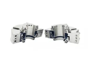
The semiconductor manufacturing involves core processes such as wafer fabrication, etching, thin film deposition, and ion implantation. Operating conditions encompass ultra-high vacuum, ultra-clean environments, highly corrosive process gases, high-frequency and high-speed rotation, and cryogenic temperature ranges. Media include highly toxic/corrosive gases such as fluorine, chlorine, silane, and ammonia. The demands for zero-leakage, ultra-cleanliness, corrosion resistance, and contamination resistance in sealing are extremely high. Traditional seals are prone to leakage, generate particulate contamination, and lack sufficient corrosion resistance, failing to meet the high-purity and high-consistency production requirements of semiconductor chips. Ferrofluid seals (magnetic fluid seals), with their core characteristics of non-contact zero wear, absolute zero leakage, no particulate generation, and resistance to extreme operating conditions, precisely address the sealing pain points of the semiconductor industry based on their own principles, becoming a core sealing solution for high-end semiconductor equipment.
Sealing Challenges
1. Rigorous Constraints of Ultra-High Vacuum and Cleanliness
Wafer manufacturing requires an ultra-high vacuum environment of 10⁻⁷ Pa or higher. Traditional seals are prone to leakage, compromising vacuum levels, leading to decreased purity of process gases and wafer oxidation. Simultaneously, particles generated from seal wear can contaminate the wafer, causing chip scrap.
2. Leakage Risk of Highly Toxic/Corrosive Process Gases
Etching and ion implantation processes use highly toxic and corrosive gases such as fluorine, chlorine, and silanes. Traditional seals are easily corroded and fail. Gas leaks not only endanger personnel safety but also pollute the production environment and damage equipment.
3. Insufficient Seal Stability Under Extreme Conditions
The production process involves alternating cryogenic and high-temperature conditions, as well as high-speed rotation. Traditional seals are prone to thermal deformation, brittleness, and liquid film instability, leading to seal failure.
4. High-precision Production Demands Interference-free Seals
Semiconductor equipment is extremely sensitive to vibration and magnetic field interference. Frictional vibration and magnetic field leakage from traditional seals can affect equipment precision, consequently impacting the consistency of chip lithography and etching.
Solutions
1. Ultra-high vacuum specialized magnetic fluid, building a solid clean sealing barrier
The magnetic fluid relies on the closed magnetic field formed by permanent magnets to firmly confine itself within the sealing gap, forming a dense "liquid sealing ring." This non-contact, frictionless process generates no particulate impurities, meeting the ultra-cleanliness requirements of semiconductors. Combined with a multi-stage toothed structure, it achieves ultra-high vacuum sealing below 10⁻⁸ Pa, completely preventing air infiltration, ensuring the purity of process gases, and avoiding wafer contamination and oxidation.
2. Corrosion-resistant specialized magnetic fluid, eliminating highly toxic gas leakage
We use a specialized carrier fluid resistant to fluorine, chlorine, and silanes. Its chemical properties are extremely stable, and it does not react with any corrosive gases used in semiconductor processes, nor does it swell or decompose. From its materials to its structure, it achieves long-term absolute zero leakage, completely blocking the leakage channels of highly toxic gases, ensuring personnel safety and a clean production environment.
3. Wide-temperature-range, high-speed adaptable magnetic fluid, stably handling extreme conditions
Customizable cryogenic-high-temperature dual adaptability, it does not solidify or volatilize under cryogenic etching and high-temperature deposition conditions, consistently maintaining stable sealing performance. Optimized viscosity and magnetization, combined with a low-loss magnetic pole structure, allow for high-speed rotation, vibration-free and magnetic field-leakage-free operation, without interfering with the precision operation of semiconductor equipment.
4. Interference-free, long-life design, suitable for high-precision continuous semiconductor production
With no mechanical wear parts, its service life under normal operating conditions is far longer than traditional seals; no flushing or lubrication systems are required, its compact structure ensures vibration-free and noise-free operation, and will not interfere with the precision of semiconductor equipment; no daily maintenance is required, significantly reducing unplanned downtime, ensuring the continuity and consistency of wafer production, and reducing maintenance costs.
① Core Operating Scenarios
• Application Scenarios: Primarily used in core processes such as wafer manufacturing, lithography, etching, ion implantation, thin film deposition (PVD/CVD/ALD), diffusion, wafer cleaning, and packaging testing. Core equipment includes single crystal furnaces, lithography machines, etching machines, coating equipment, wafer transfer robots, vacuum chambers, molecular pumps, valves, and other key rotating shafts and dynamic sealing components. Key Pain Points:
• Extremely high vacuum requirements: Semiconductor processes need to achieve ultra-high vacuum levels above 10⁻⁸ Pa. Traditional seals suffer from gas release and micro-leakage, making it impossible to maintain a stable ultra-high vacuum environment, leading to process failures and wafer scrap.
• Nanoscale cleanliness requirements: Traditional seals are prone to wear and shedding, and the resulting micron/nanoscale particles can contaminate wafers, causing circuit defects and a significant decrease in yield.
• Processes involve highly corrosive and toxic electronic specialty gases such as chlorine, hydrogen fluoride, and boron trifluoride. Traditional seals are prone to corrosion and aging, leading to gas leaks, which causes safety accidents and equipment damage
• Wide process temperature ranges: Traditional seals are susceptible to thermal expansion and contraction, causing seal failure.
• Equipment requires 24/7 uninterrupted stable operation. Traditional seals have short lifespans, requiring frequent replacement and maintenance, resulting in significant downtime losses. Furthermore, imported seals have long lead times, high costs, and slow service response times.
② Product Highlights
• Ultra-high vacuum with zero leakage: Utilizing a semiconductor-grade ultra-low outgassing magnetic liquid formula and precision sealing structure, it achieves absolute zero leakage in ultra-high vacuum environments, with an ultimate vacuum level reaching 10⁻⁹ Pa. This fully meets the ultra-high vacuum requirements of the entire semiconductor wafer manufacturing process, and its vacuum stability far surpasses that of traditional seals.
• Ultra-clean and contamination-free: Zero friction, zero wear, and no chip shedding design eliminates particulate matter release. Combined with semiconductor-grade clean materials, it completely eliminates the risk of particulate contamination, meeting the production requirements of Class 1 cleanrooms and ensuring wafer yield.
• Strong corrosion and specialty gas resistance: A customized magnetic liquid formula and sealing structure resistant to highly corrosive electronic specialty gases allow for long-term tolerance to highly corrosive and toxic specialty gases commonly used in semiconductor processes, such as hydrogen fluoride and chlorine. This solves the pain points of traditional seals, which are prone to corrosion, aging, and rapid failure.
• Wide temperature range and high stability: Perfectly adapted to the high and low temperature alternating conditions of semiconductor processes, with minimal thermal deformation and long-term stable sealing performance without degradation.
• Long lifespan and maintenance-free: Flexible contact sealing structure with zero friction and wear, offering a service life of over 2 years. Maintenance-free operation far exceeds traditional seals, significantly reducing equipment downtime and lowering overall operating costs.
• Controllable domestic substitution: Completely independently developed and manufactured, with controllable delivery times and rapid service response, breaking the monopoly of foreign brands, facilitating domestic substitution of semiconductor equipment, and ensuring supply chain security.
• Full process customization: Customized ultra-high vacuum clean sealing solutions can be tailored to different semiconductor process stages, equipment specifications, and operating conditions, adapting to applications ranging from R&D-level pilot equipment to 12-inch wafer mass production lines.
Customer Application Cases
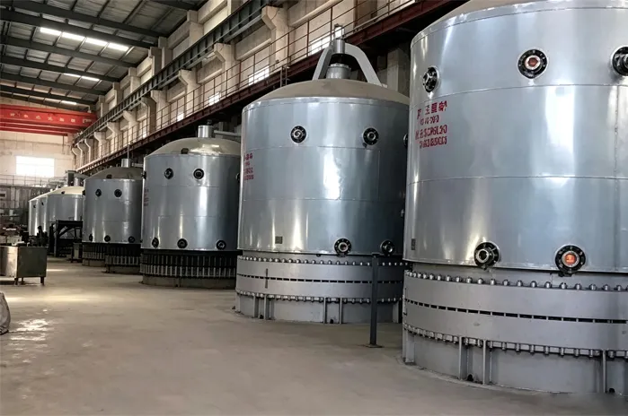
Shanghai Yunsheng High-Purity Silicon Project:
 English
  français
  Español
  العربية
  русский